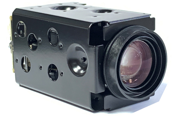
Hi3516C HD camera solution

Product Name: Smart HD IP Camera
Industry: Industrial Internet of Things
Main Chips: Hi3516C, H5AN4G6NAFR-UHI, RTL8201FI-VC-CG, ICL3232EIA_T, MX25L25635
Board Type:
Application Area: Automation Equipment Vision Control, Robot Motherboards
Pin Count: 1753
Layer Number: 8
Board Thickness: 1.6mm
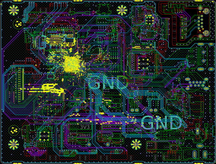
Dimension: 145.55*137.09 mm
Line Width/Spacing: 4/4mil
| Product Name | Smart HD IP Camera |
| Industry | Industrial Internet of Things |
| Main Chips | Hi3516C, H5AN4G6NAFR-UHI, RTL8201FI-VC-CG, ICL3232EIA_T, MX25L25635 |
| Board Type | |
| Application Area | Automation Equipment Vision Control, Robot Motherboards |
| Pin Count | 1753 |
| Layer Number | 8 |
| Board Thickness | 1.6mm |
| Dimension | 145.55*137.09 mm |
| Line Width/Spacing | 4/4mil |
| Design Challenges | 1. Small PCB size causing layout difficulties, such as SD card, network port, audio, MIPI interface, all need to consider the main chip's wiring position. 2. Signal interference, PCB heat dissipation. 3. Differential driving circuit. 4. Whole machine ESD design. |
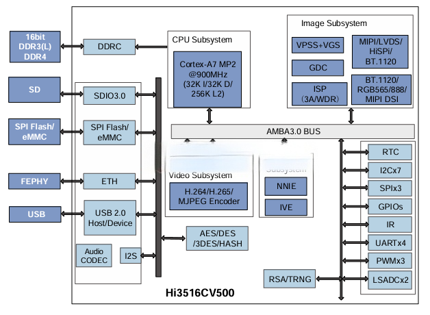
One: Hi3516C Chip Functional Structure Diagram:
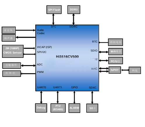
Camera Solution:
Two: Partial Schematic Design Display:
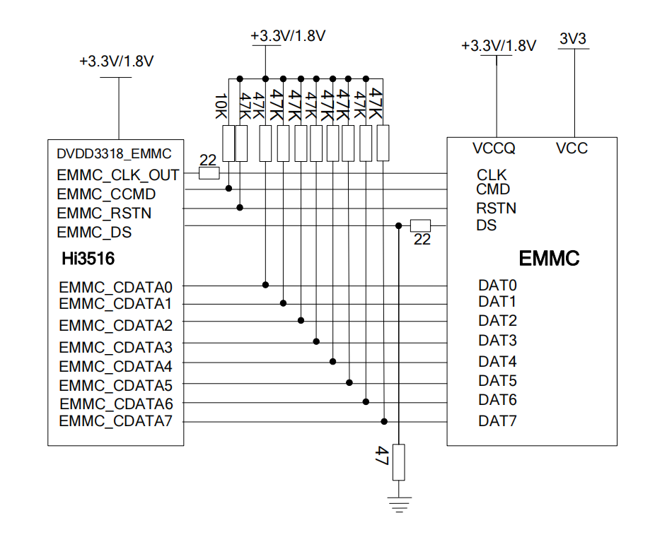
1 EMMC
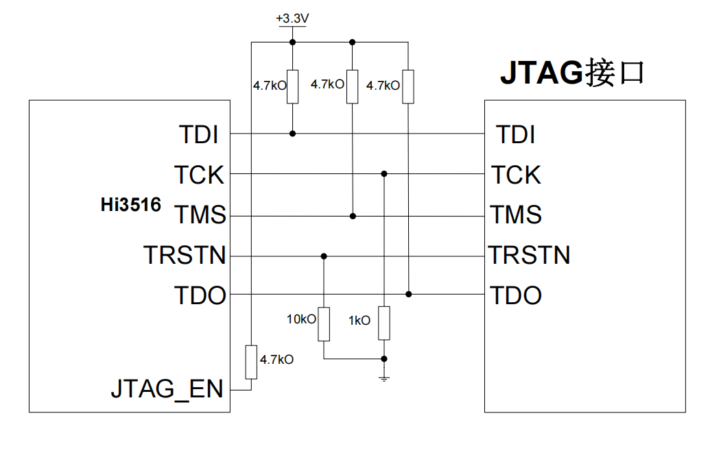
2 JTAG
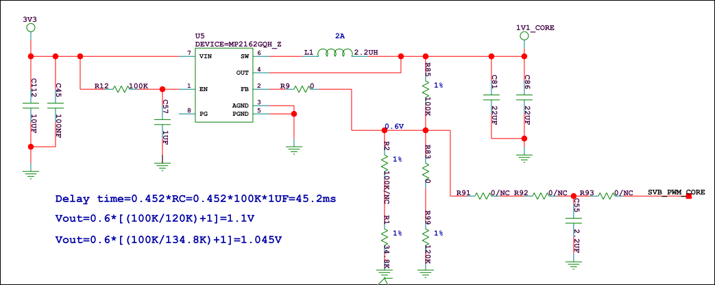
3 Core Power Supply Schematic
Three: Partial Layout Details Display
1: DDR Power Section Design
Hi3518EV20X's DDR_I/O power pins need to be placed close to decoupling capacitors, and there should be at least one 10μF ground filtering capacitor on the DDR_I/O power channel.
DDR_Vref reference voltage design strategy: To reduce DDR_Vref noise, the DDR_Vref power module should be connected directly to the chip's DDR_Vref BALL with wide traces on the TOP layer, and the power module should be placed close to the chip pins.
DDR_PLL power design strategy is as follows:
A: When designing DDR_PLL power, it must be isolated from other power sources using magnetic beads (1KΩ @100Mhz)
B: Decoupling capacitors of DDR_PLL power should not share ground vias with other components.
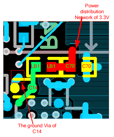
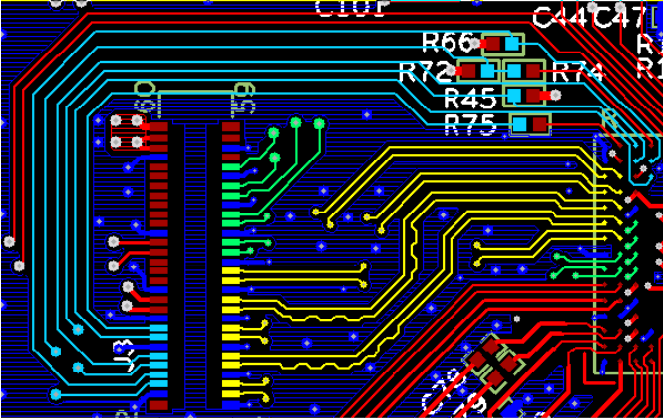
2: PCB Design of MIC_BIAS for Dual MIC Input
a. Yellow for audio input signal, white for audio output signal, green for MIC_bias signal, and blue for ground copper. The surface traces reference the GND layer and are isolated from nearby high-speed digital signals.
3: PCB Design of Audio Input/Output Signal Lines
Yellow for audio input signal, white for audio output signal, green for MIC_bias signal, and blue for ground copper. The surface traces reference the GND layer and are isolated from high-speed digital signals.
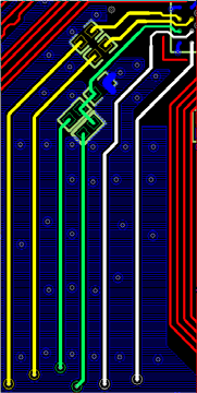
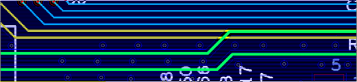
4: PCB Design for Isolating Audio Signal Lines from Other High-Speed Signal Lines
Green for audio traces (Top layer), blue for SDIO module high-speed digital signal lines, yellow for SDIO module low-speed signal lines (Bottom layer), there are ground vias between yellow audio traces and green audio traces, isolating audio signal lines from other high-speed signal lines.
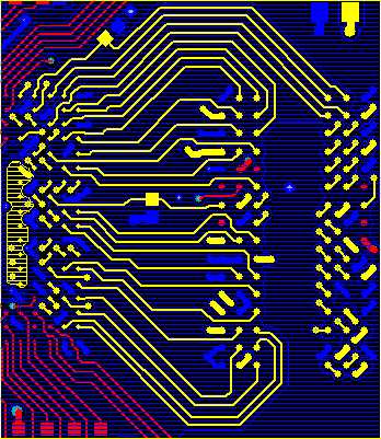
5: VI Interface Design Requirements for Compatible Differential and Single-ended Interface Sensors
A: Requirement for VI PCB design, 5 pairs of signals named MIPI should be differential (controlled within ±5mil in length and ±100mil based on clock signals), impedance control within 100Ω ± 10% for differential pairs, and 50Ω ±10% for other signals, with trace spacing following the "3W" principle.
B: VI interface has 1.8V and 3.3V power domains, ensure reference power planes for avoiding impedance mismatch, data lines, row sync, field sync signals, SPI0 on the top layer using ground plane as reference.
C: VI interface selects 1.8V power domain, signal trace length should not exceed 4 inches.
 Yellow signal lines denote 5 pairs of differential MIPI interface lines, green for other single-ended data signal lines, light blue for Sensor configuration interfaces, reset and clock signals.
6: DDR Routing Design, including line width, spacing, length, grounding, filtering, should strictly follow hardware design parameters, external resistors for DDR chips must be precise ±1% 240Ω resistors.
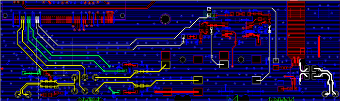
TOP Layer Signal Routing Design
BOTTOM Layer Signal Design
Four: Component Layout
Consider the product structure and heat dissipation in the layout strategy:
a. Distribute high-power components evenly on the single board to avoid local overheating that affects component reliability.
b. Hi3516 and power components should be placed close to the positioning holes to dissipate heat through screw holes and chassis to the external environment.
c. Place thermally sensitive devices (Sensors, Flash, etc.) away from high-power components to minimize the impact of heat, preventing overheating that affects system stability and image quality.
d. Expose copper on as many PCB screw holes as possible for better contact between PCB and chassis.
Five: Routing Heat Design Strategy
a. Use FULL via connections for the chip to improve heat dissipation efficiency.
b. Connect Hi3516's 1.1V/1.8V/3.3V power and ground pins with copper layers, add as many vias as possible on these copper layers to connect to power and ground planes, enhancing chip heat dissipation.
Six: Full Layout Display
Design Application:
Related Products


-
 Rapid Prototyping
Providing comprehensive one-stop PCB service solutions
-
 Payment Security
Multiple payment channels to ensure customer payment security!
-
 Fast Delivery
Fastest 8 hours, small batch speed 1-2 days
-
 Quality Assurance
If the quality does not match the description or has defects, we will refund.
