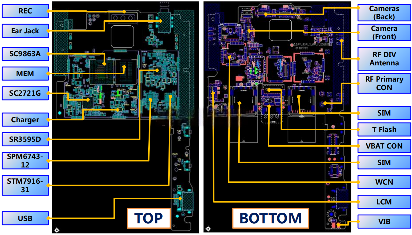
Unisoc SC9863A RTK Tablet PCB Design

Product Name: Industrial RTK Handheld
Industry: Communication Products
Operating System: Android 9.0
Main Chips: Spreadtrum SC9863A (CPU)
Board Type: RTK Handheld Motherboard
Pin Count: 5101
Layer Number: 8
Signal Rate: No Limit
| Product Name | Industrial RTK Handheld |
| Industry | Communication Products |
| Operating System | Android 9.0 |
| Main Chips | Spreadtrum SC9863A (CPU) |
| Board Type | RTK Handheld Motherboard |
| Pin Count | 5101 |
| Layer Number | 8 |
| Signal Rate | No Limit |
SC9863A Package Dimension Data-1
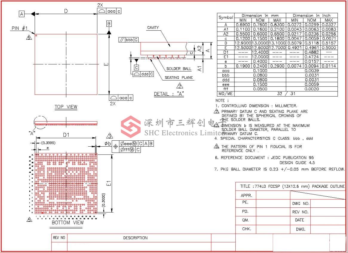
SC9863A Package Dimension Data--2
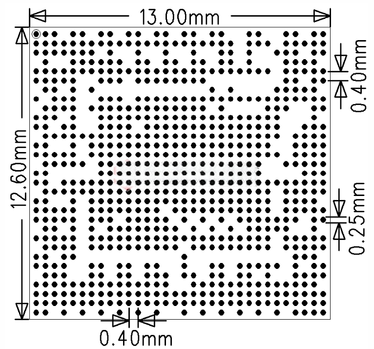
SC9863A Component Package
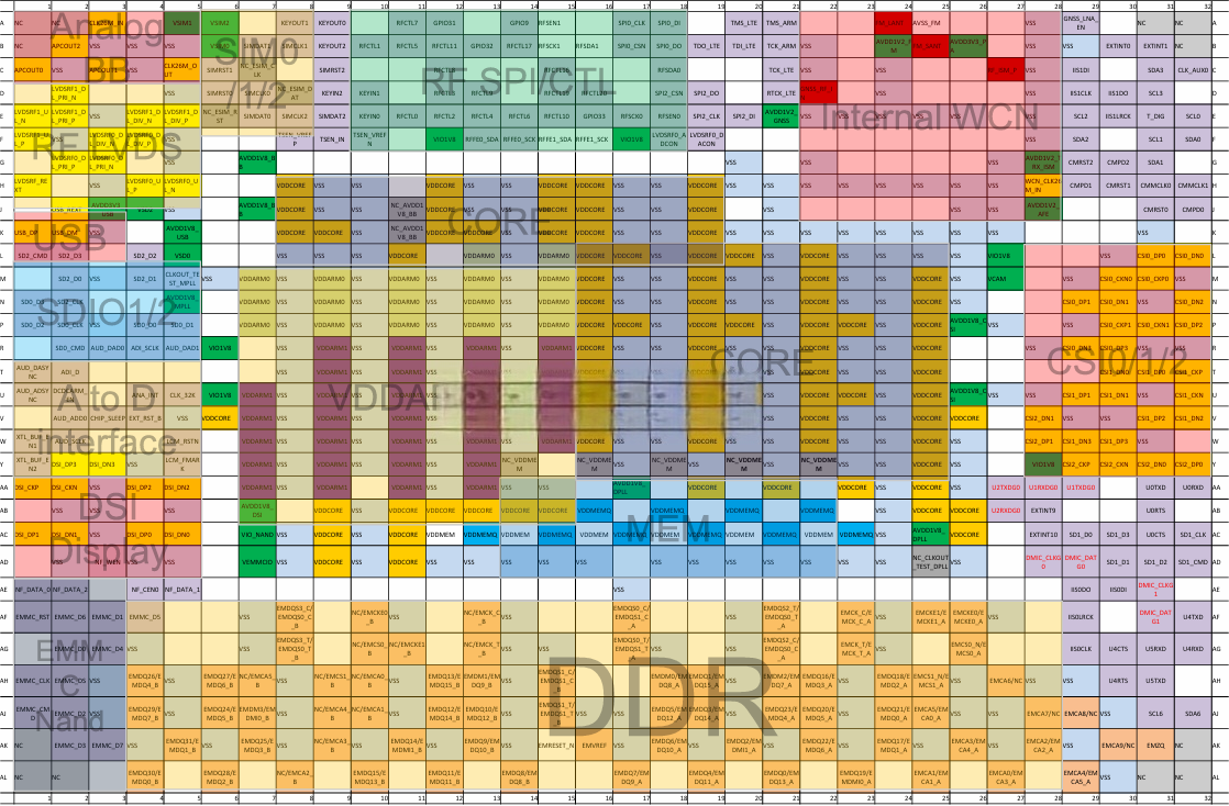
SC9863A BGA Pin Definition
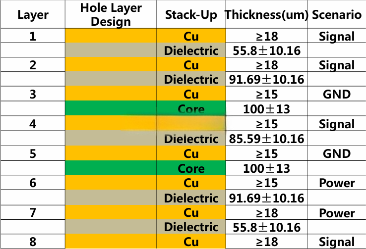
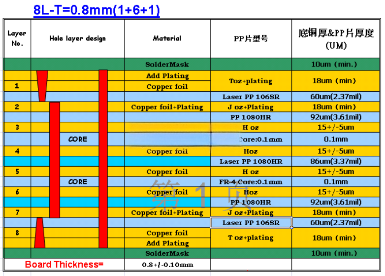
PCB Design Stack Notice
SC9863A placement supports double-sided only. The minimum PCB stack is 8HDI-1.
PCB total thickness is recommended to be around 0.8mm ±10%.
Utilize recommended PCB stack-ups as much as possible to optimize electrical performance by adjusting PCB thickness and materials.
Implement specific allocations on LPDDR3 and BB PCB domains.
Reference PCB stack-up is illustrated as follows: - 8HDI-1 (1+6+1).
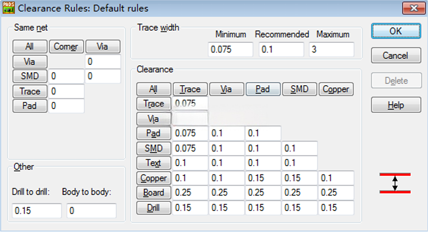
General Design Parameters
Laser Via Parameters Setting
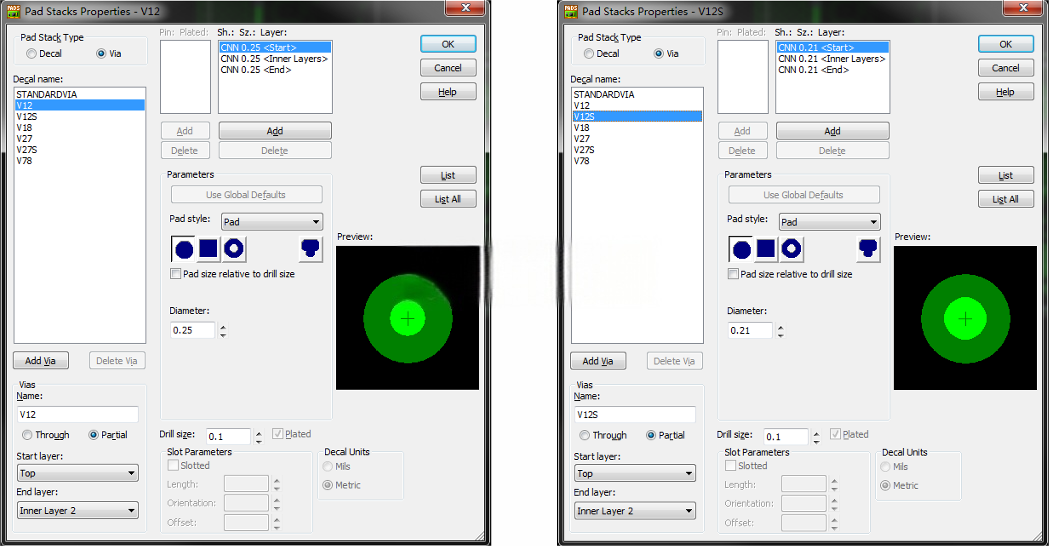
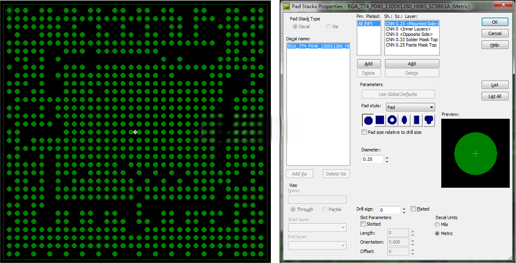
Laser via: Drill hole diameter 0.1mm, pad diameter 0.25mm.
Laser via (RF dedicated): Drill hole diameter 0.1mm, pad diameter 0.21mm.
Buried Via Parameters Setting
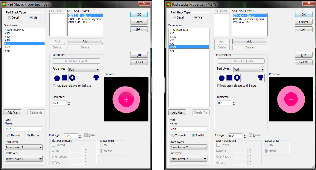
Buried via method: Hole diameter 0.25mm, pad diameter 0.45mm.
RF buried via method: Hole diameter 0.2mm, pad diameter 0.4mm.
PCB Design Rules - Fanout Control
Recommended Layout
Layout Priority
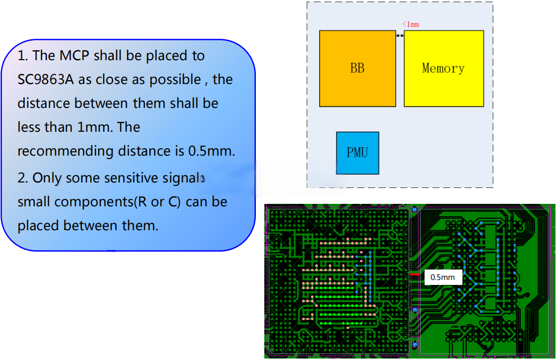
1. Obtain a good DDR SI and PI by reusing SPM based on PCB outline and stack-up.
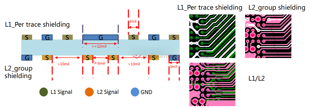
2. Design sensitive RF traces and interference zones with shielding.
3. Layout and distribution of 26MHz/32K clock signals.
4. Layout and distribution of high-speed signals (MIPI, LVDS) (Note: at least one GND reference plane, impedance control).
5. Layout and distribution of audio signal traces (Note: isolate GND plane integrity).
6. Layout and distribution of DC-DC switch power and LDO traces.
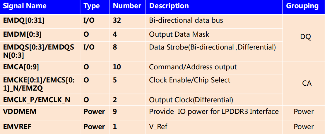
SC9863A LPDDR3 BGA Pinout Sequence
Design Requirements:
1. SC9863A LPDDR3 can support 1866Mbps, so PCB layout must strictly follow the final actual SI and PI simulation results.
2. To ensure the best SI quality and PDN, it is necessary to reuse SPM as a reference for PCB layout design.
LPDDR3 Layout Rules
1. Below SC9863A, routes may follow the 3mil/3mil rule;
2. Do not overlap signal traces on different layers (L1/L2), choose orthogonal or staggered as much as possible. Connect BB to eMCP.
3. Maintain the same solid reference plane on top and bottom of signals, preferably GND plane. Keep the thickness between signal and reference plane as short as possible. Connect L1 and L2 GND shields through tiny vias, reduce crosstalk by connecting L2 and L3 GND shields near BB and eMCP ranges.
4. LPDDR3 clock frequency is 933MHz.
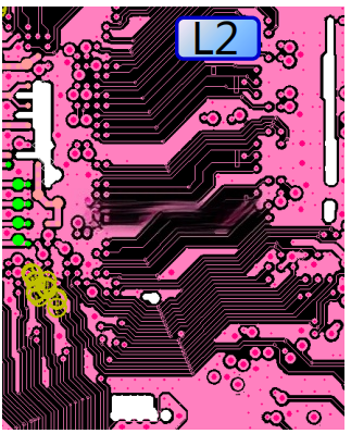
Routing Requirements (as shown in the figure below)
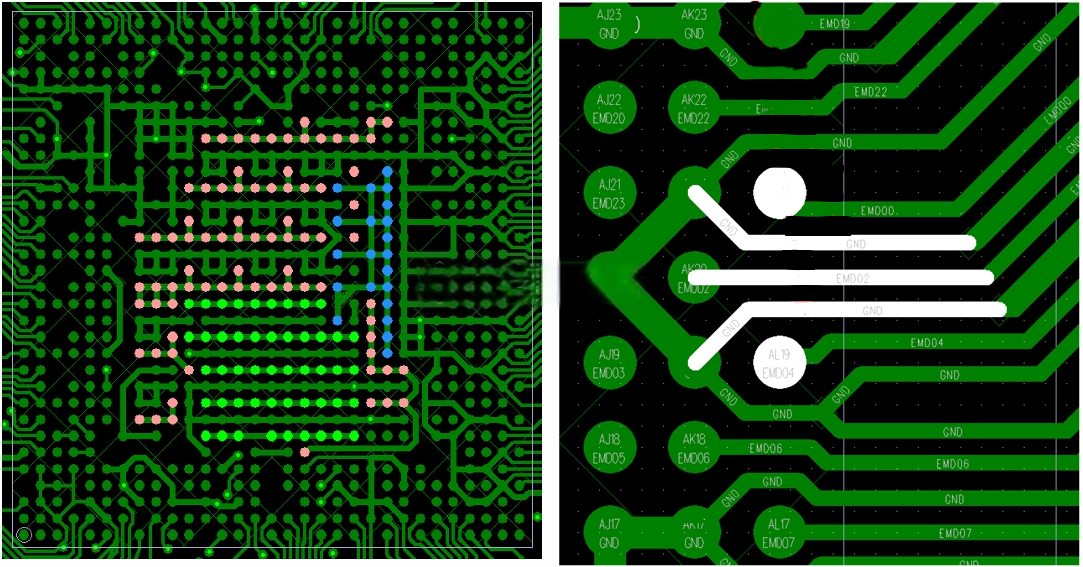
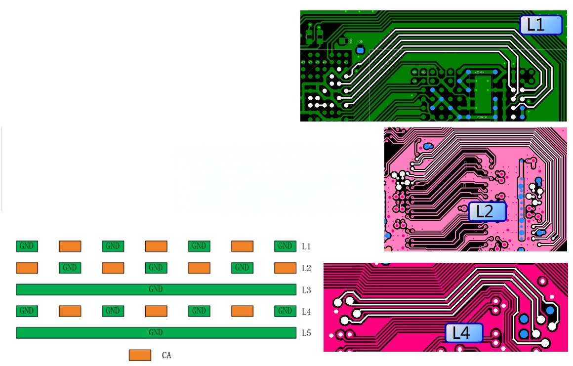
1. Route all DQ/DM traces on the first and second layers and maintain a complete GND reference on the third layer.
2. Keep traces as short as possible, |DQS-DQ|≤7mm, |DQS-DM|≤7mm.
3. Maintain DQ/DM traces with GND shield on L1; alternate signal on L1 and L2; ensure spacing between every two traces on L2 as shown in the figure. Connect GND shields of L1/2 and L2/3 with vias at both ends.
4. Reserve L3 as a complete reference GND plane and L6 as VDDMEM power plane.
CA Signal Line Design
Routing Requirements
1. Route all CA traces on L1, L2, and L4, each trace should be shielded with GND as short as possible, |CLK-CA|≤7mm, alternate paths on L1 and L2 for all CA signals.
2. Connection of GND shield layers of L1/2 and L2/3 with vias at both ends to reduce crosstalk. Prefer more vias.
CLK/DQS Design Requirements:
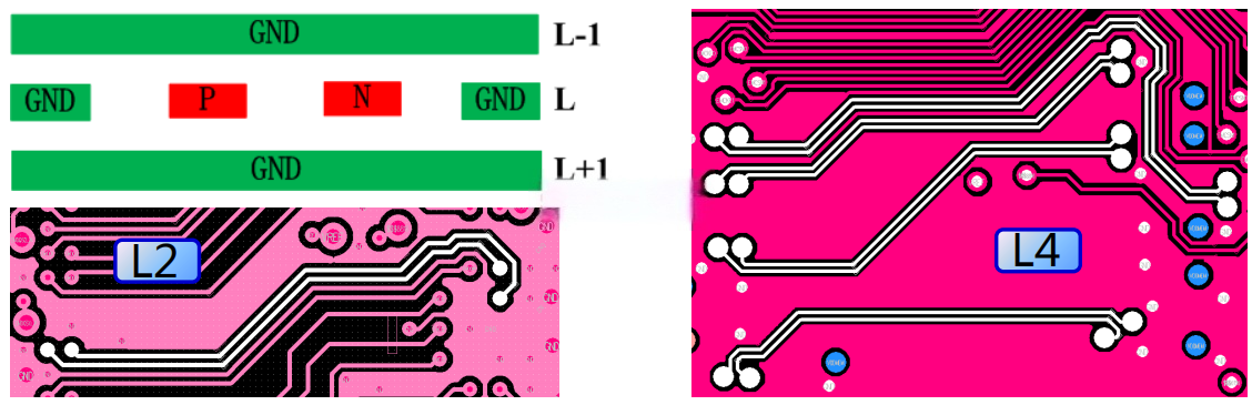
1. CLK/DQS should comply with the differential pair routing rules, keep P/N parallel lines, |DQSP - DQSN|≤1mm, |CLKDP - CLKDM|≤1mm;
2. Trace width/spacing: W/S=3mil/3mil (as shown in the figure);
3. For 8L PCBs, keep solid GND planes for L3 and L5 for differential pairs, for pairs at L3, maintain solid GND plane for 2L;
4. Maintain thorough cuts to form power and ground loop channels for 8L PCBs;
5. Use GND (adjacent and upper/lower layers) shields.
PCB Power Layer Design Requirements
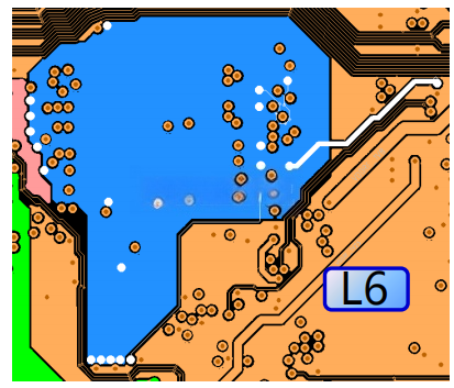
1. VDDMEM power plane is mandatory, this layer must cover all LPDDR3 signals and SC9863A pins.
2. Power planes must have a comprehensive reference ground plane, with minimal distance between them.
3. Power vias and GND vias must be arranged in a rectangular layout, with an optimal ratio of 1:1. GND vias must be close to power vias to reduce loop inductance.
4. Connect the power plane to SC9863A's VDDMEM ball using at least 10 blind vias and 5 buried vias.
Keep the entire GND plane below or above the power planes, minimizing the distance between the two planes. Overlap method as follows:
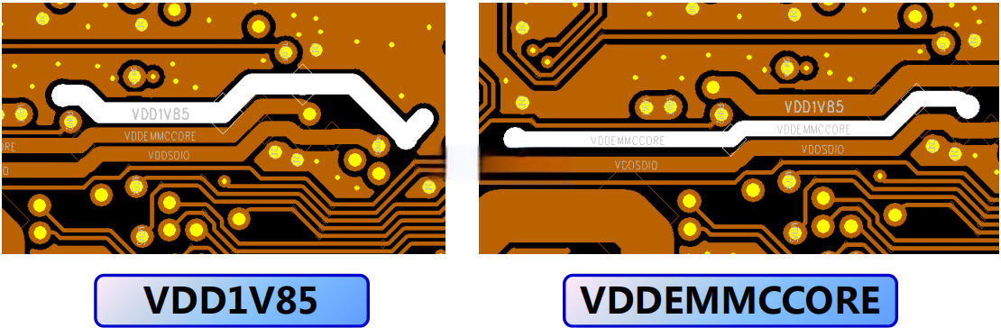
The width of VDD1V85 should be no less than 0.4mm. The width of the core should not be less than 0.3mm.
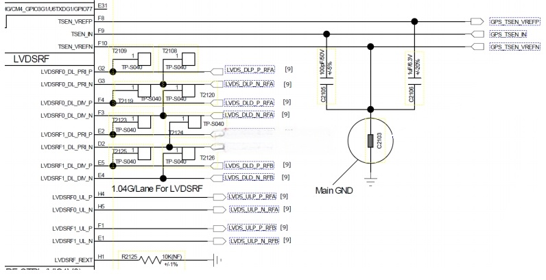
RF Transceiver TSX-GND Design Schematic
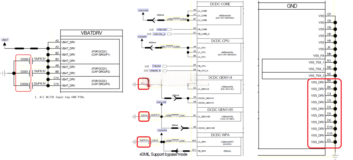
VBAT Power Design
VBAT_DRV pin in SC2721G ball map is divided into three parts, each part should be directly connected to a 10uF capacitor.
Trunk trace width should not be less than 0.5mm. Impedance characteristics of each part should meet the target impedance.
Do not connect VBAT_DRV pins to other VBAT pins.
All DC/DC input capacitor ground pads should be isolated from all other ground planes and have dedicated vias to the main ground plane.
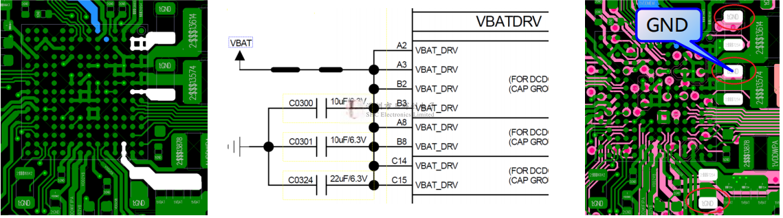
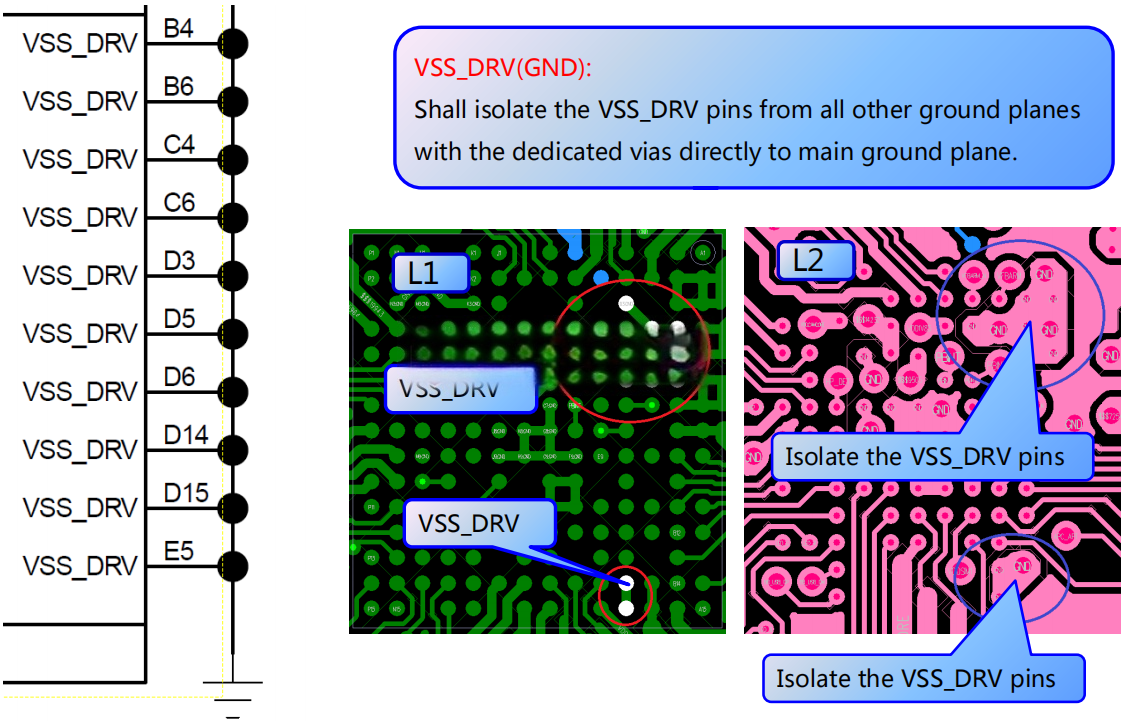
SC2721G DC-DC Isolation to Main GND Network Schematic
RF Transceiver SR3595D Schematic and Circuit
Actual Product Application Images RTK Handbook
Related Products


-
 Rapid Prototyping
Providing comprehensive one-stop PCB service solutions
-
 Payment Security
Multiple payment channels to ensure customer payment security!
-
 Fast Delivery
Fastest 8 hours, small batch speed 1-2 days
-
 Quality Assurance
If the quality does not match the description or has defects, we will refund.
