HiSilicon Hi3403 Intelligent Image Processing Motherboard

Product Name: AI ISP Intelligent Image Processing Motherboard
Industry: Industrial Internet of Things
Main Chips: Hi3403-SS928, H26M41204HPR, K4UBE3D4AA-MGCL000, RTL8211FI-CG, SGM6505HYTQF24G_TR
Board Type: Motherboard
Application Area: Automation Equipment Vision Algorithm Motherboard, Drone Application Fields
Pin Count: 4634
Layer Number: 8
Board Thickness: 1.6mm
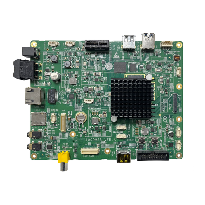
Dimension: 165*143 mm
Line Width/Spacing: 4/4mil
Component Quantity: 1084pcs
| Product Name | AI ISP Intelligent Image Processing Motherboard |
| Industry | Industrial Internet of Things |
| Main Chips | Hi3403-SS928, H26M41204HPR, K4UBE3D4AA-MGCL000, RTL8211FI-CG, SGM6505HYTQF24G_TR |
| Board Type | Motherboard |
| Application Area | Automation Equipment Vision Algorithm Motherboard, Drone Application Fields |
| Pin Count | 4634 |
| Layer Number | 8 |
| Board Thickness | 1.6mm |
| Dimension | 165*143 mm |
| Line Width/Spacing | 4/4mil |
| Component Quantity | 1084pcs |
| Design Challenges | 1. Signal interference. 2. Differential driving circuit. 3. Numerous types of power supplies, high current flow, limited vertical channels. 4. High signal speed (DDR5/PCIE5.0 etc.), limited trace length. |
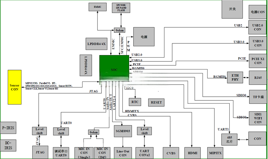
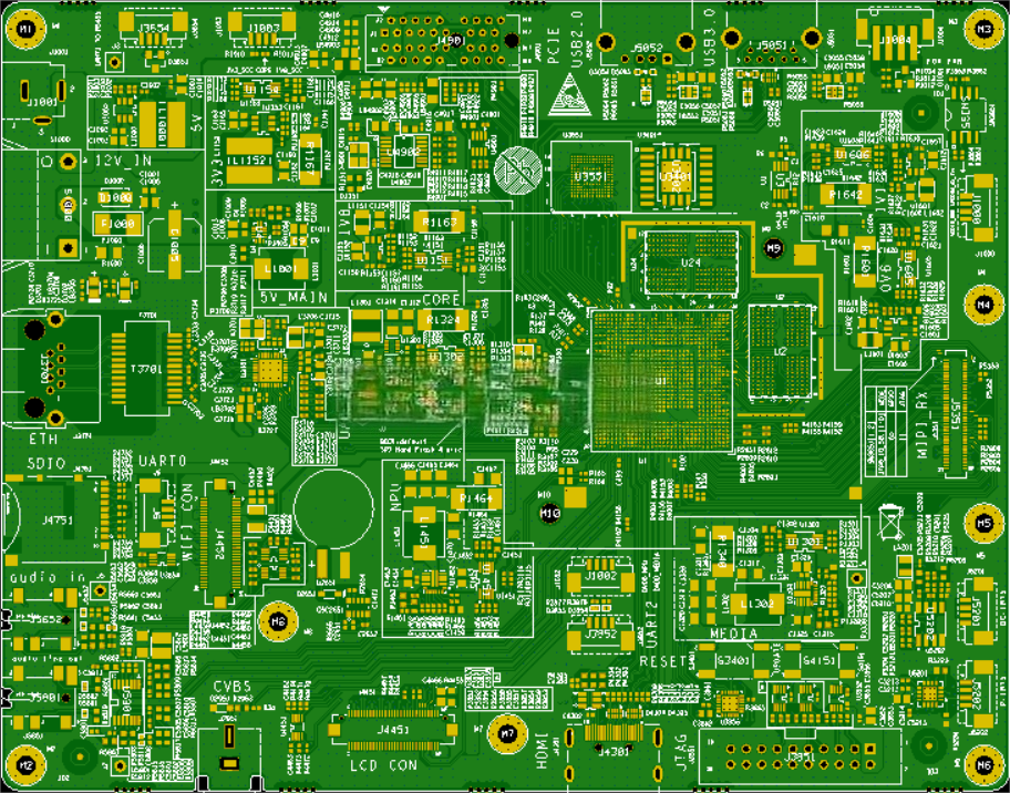
Hi3403-SS928 Chip Functional Structure Diagram :
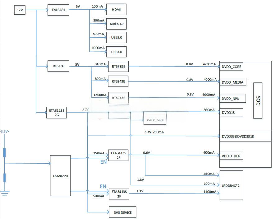
Power Tree
Partial Schematic Design Display :
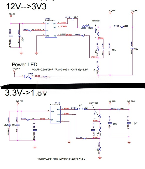
1. Power Supply Schematic
12V to 3.3V, 3.3V to 1.8V
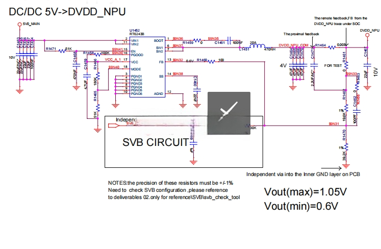
DVDD-NPU
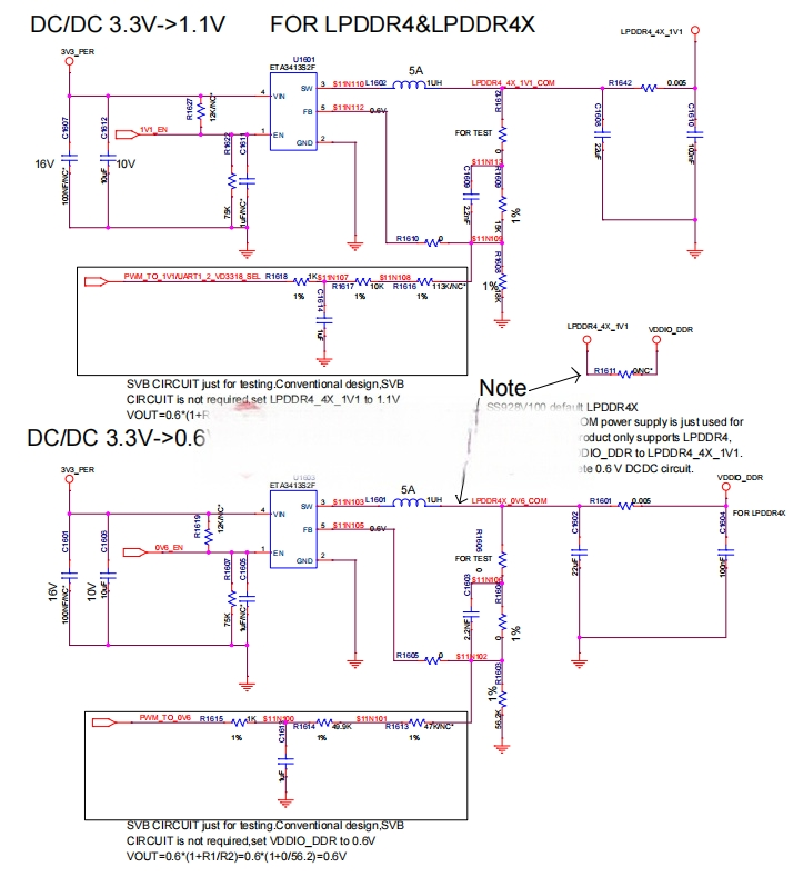
DC/DC 3.3V to 1.1V 3.3V to 0.6V (LPDDR4 Power Supply Part)
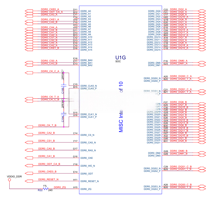
2. DDR4
3. SYS Schematic
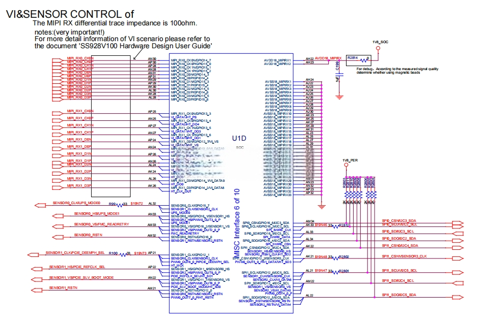
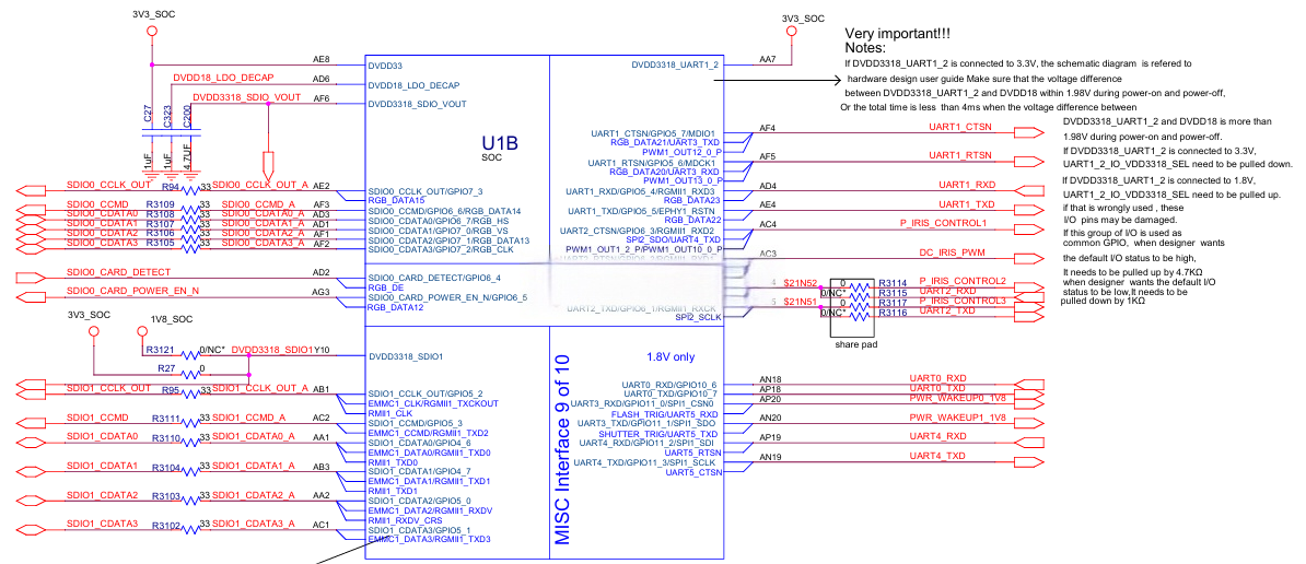
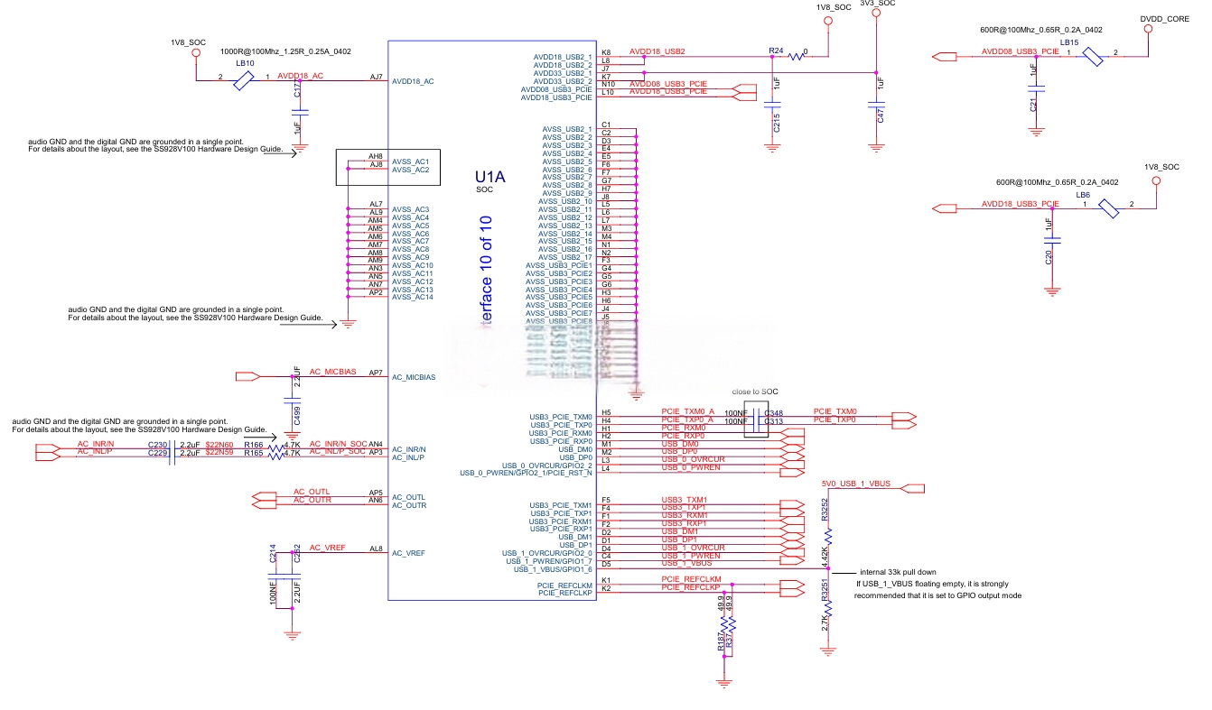
4. VI & Sensor Control Schematic
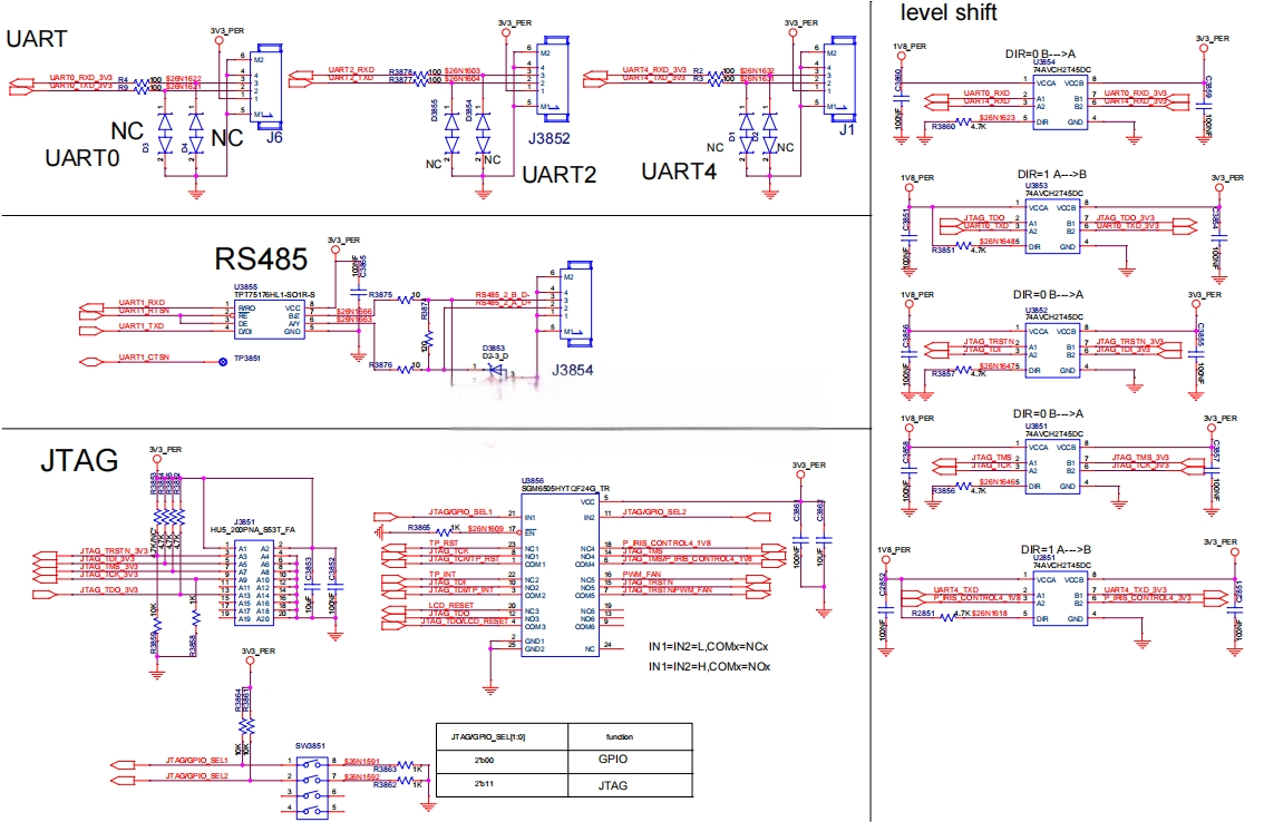
5. Peripheral
1:
2:
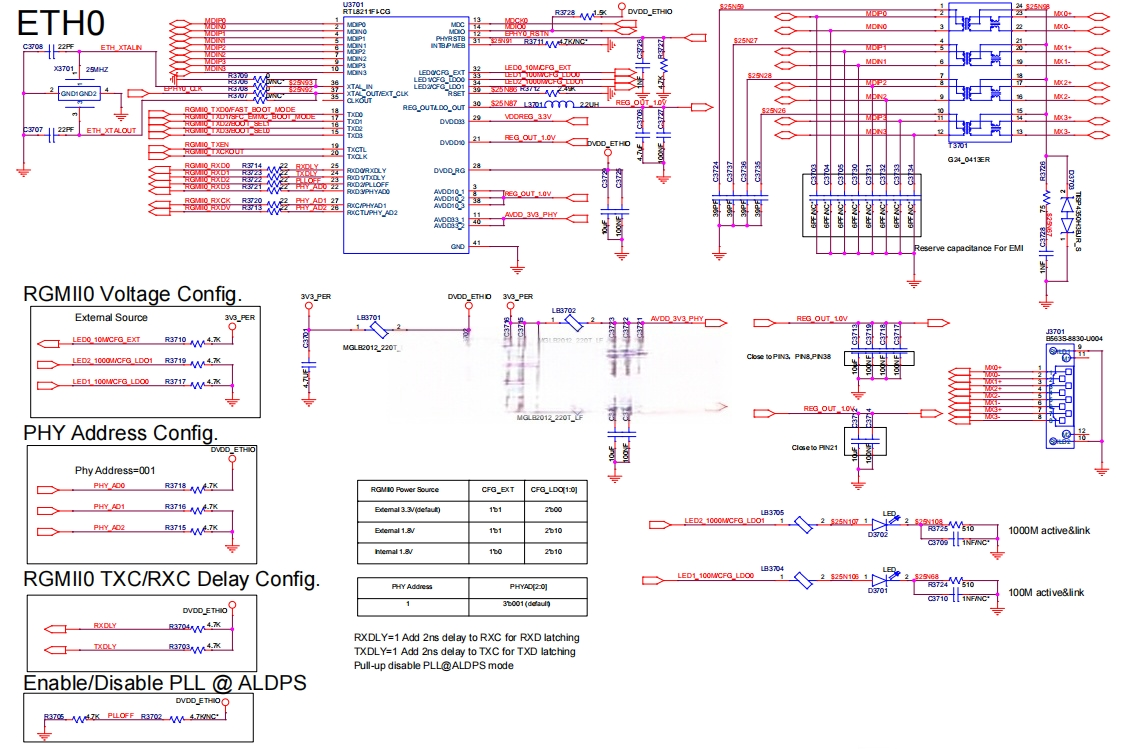
6. Ethernet Port
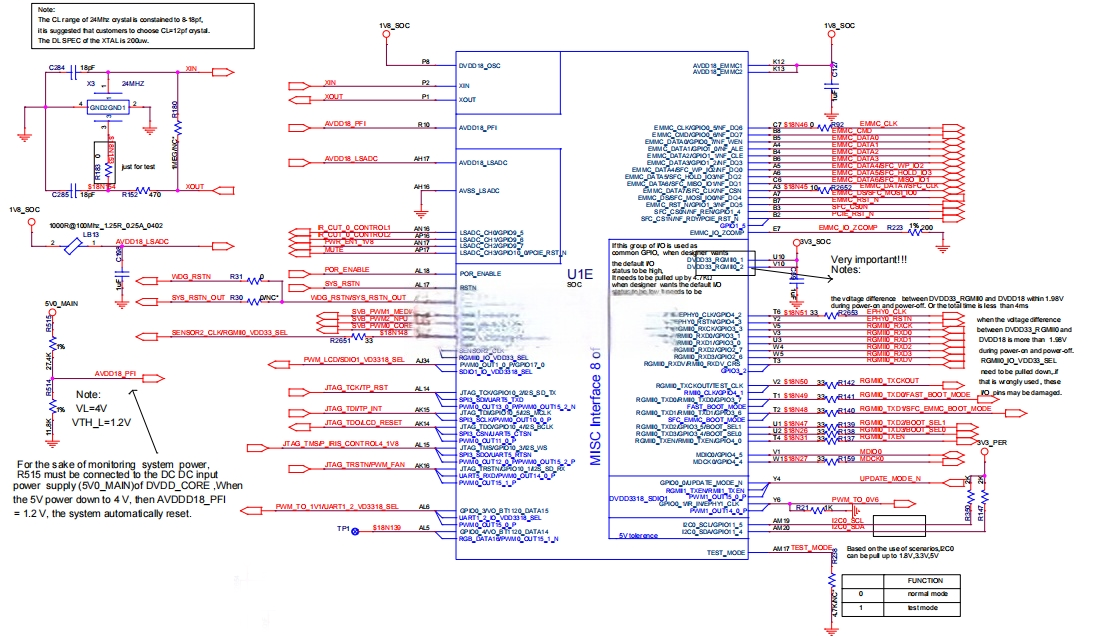
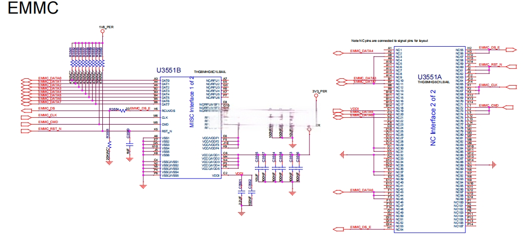
7. EMMC
8. UART & JTAG
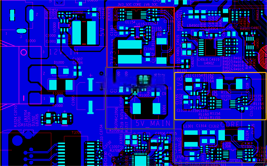
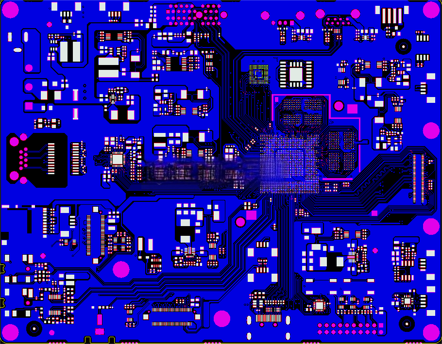
Partial Layout Details Display
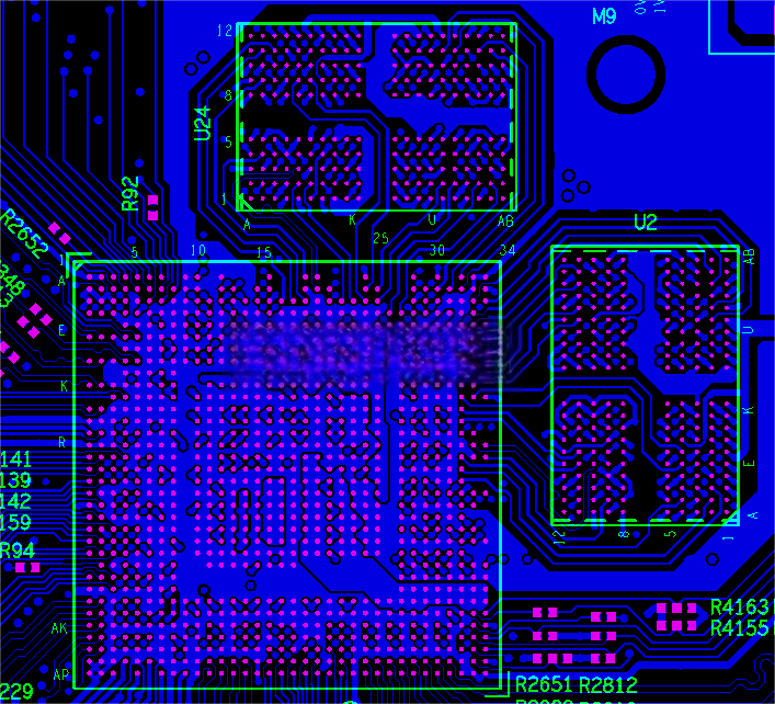
1: Layout of CPU and Memory, high signal rate, using high-speed board design (Synamic 6GX), with 10-degree wiring; combined with simulation results to optimize signal via holes, pads, etc., and increase reflow ground holes;
2: Due to limited vertical channels on the single board, 12V needs to flow from top to bottom. Two 2OZ power layers are stacked; 12V is segmented from the power layer to meet the current requirements downstream;
3: The power module layout is compact, placed near the load end, positioned above and below the CPU and DIMM; a high-speed line channel is left in the middle of the single board to avoid high-speed lines penetrating the power module;
Distribution of CPU and K4UBE3D4AA-MGCL, considering overall signal transmission.
GND layout, CORE power, aside from the power layer plane, reinforced from the routing layer for high-current components, in coordination with SI simulation, to meet current flow and voltage drop requirements;
Signal Transmission Layer: Due to many high-speed lines, the wiring layer closest to the TOP layer is used, with back-drilling design to meet signal quality requirements;
Power Supply Part Design
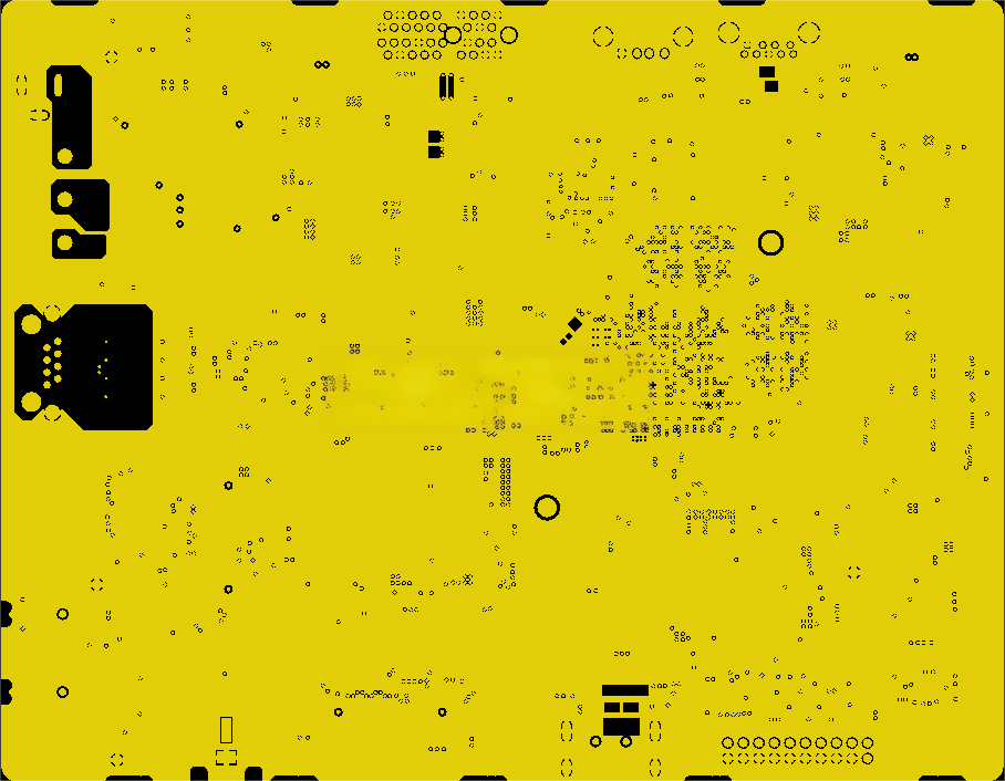
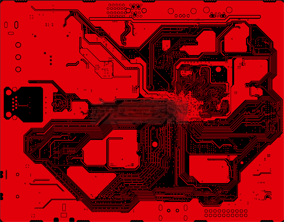
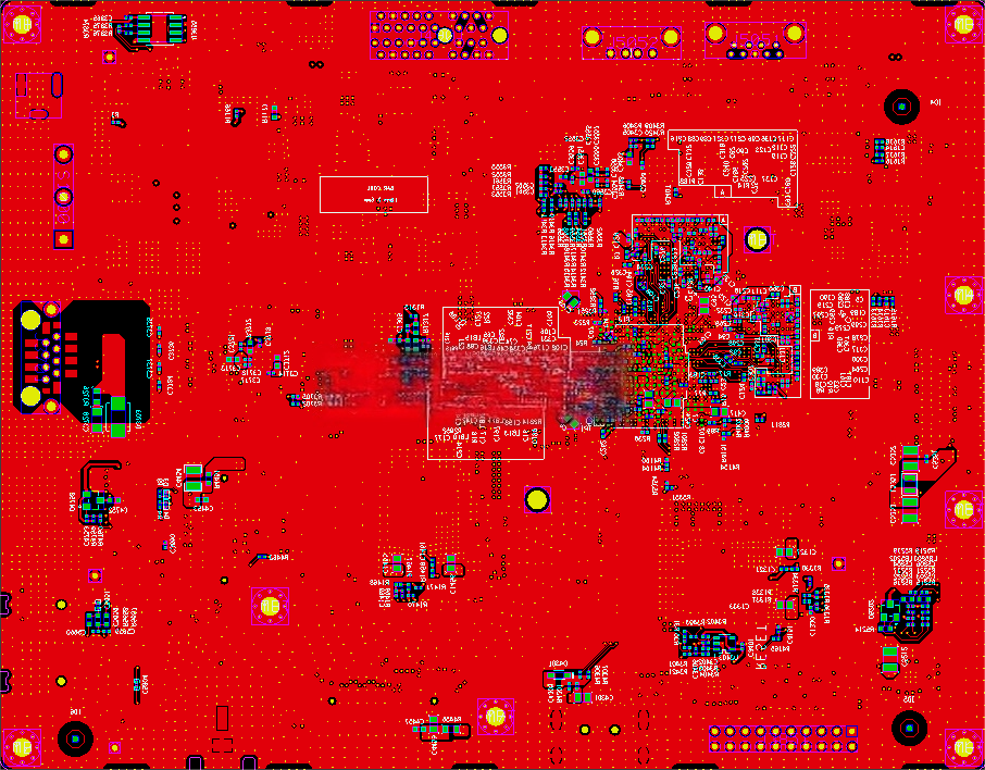
Full Layout Display
PCB Images:
Application:
Related Products


-
 Rapid Prototyping
Providing comprehensive one-stop PCB service solutions
-
 Payment
Security
Payment
Security
Multiple payment channels to ensure customer payment security!
-
 Fast
Delivery
Fast
Delivery
Fastest 8 hours, small batch speed 1-2 days
-
 Quality
Assurance
Quality
Assurance
If the quality does not match the description or has defects, we will refund.