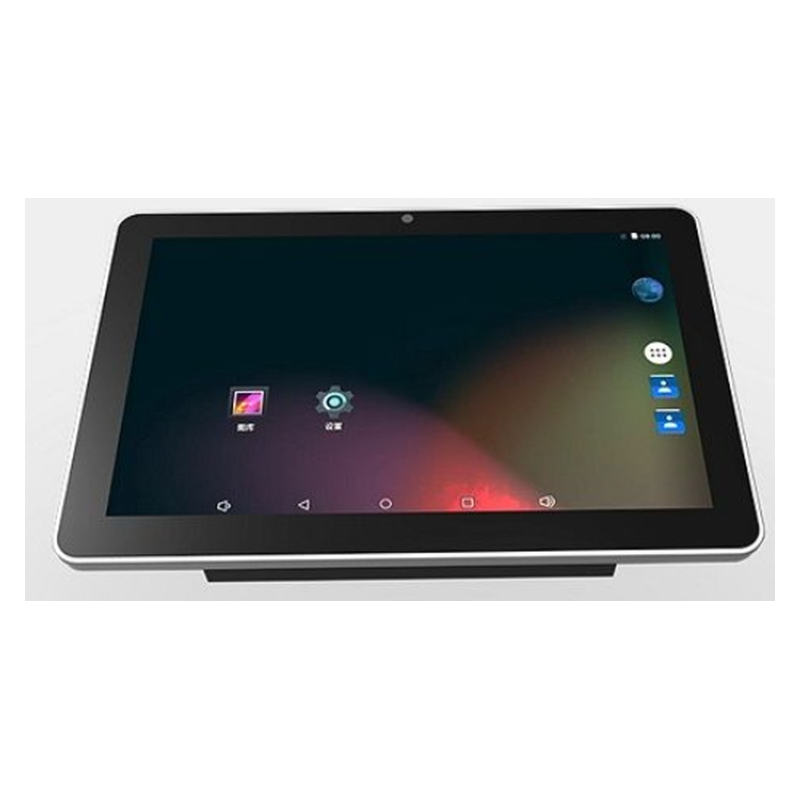
Rockchip RK3288 tablet solution (6 layers)

Product Name: Rockchip RK3288 Tablet
Industry: Communication Products
Compatible System: Android 10.0
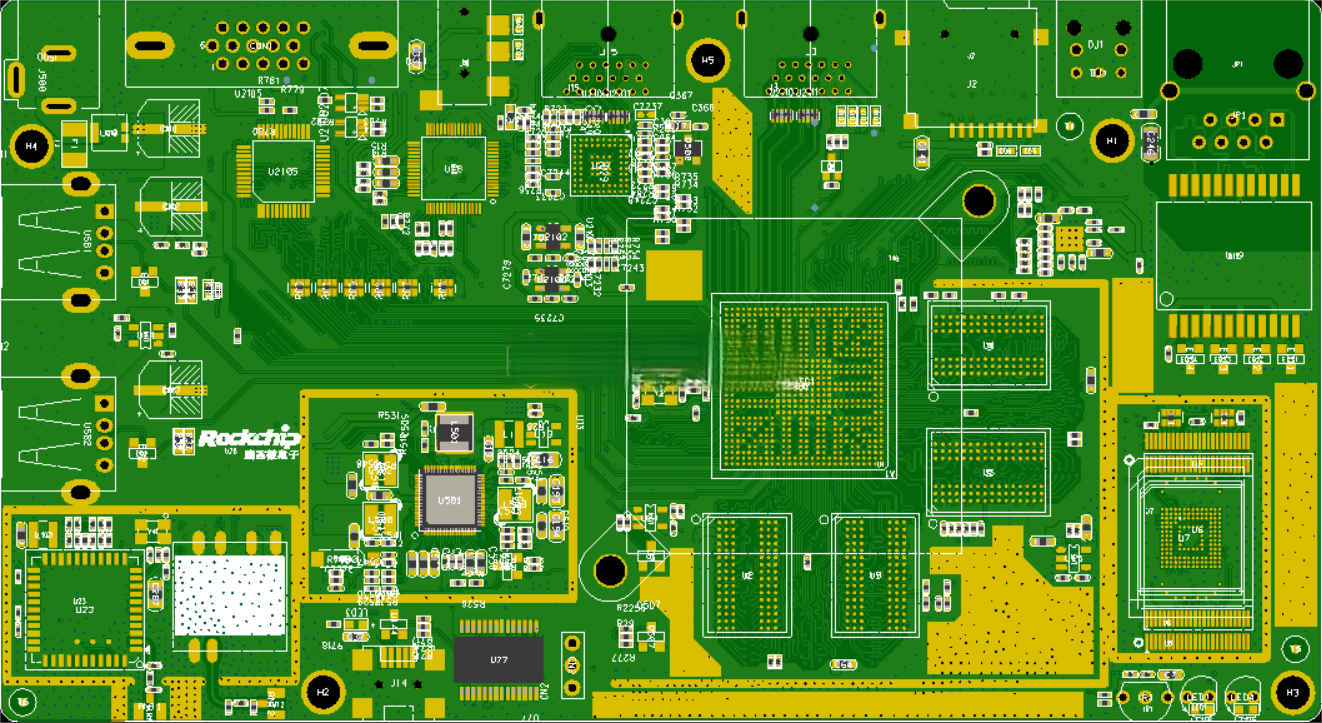
Main Chips: MCU_RK3288, DDR3_128MX16BIT*4 (64G), EMMC, RK1000-S, TC358749XBG, DRV632PW, FT232RL, RK808-B, SDA7123
Board Type: Tablet Computer Motherboard
Application Area: Industrial Tablet Computer
Pin Count: 3717
Layer Number: 6
Board Thickness: 1mm
Dimension: 150*82mm
Line Width/Spacing: 4/4mil
| Product Name | Rockchip RK3288 Tablet |
| Industry | Communication Products |
| Compatible System | Android 10.0 |
| Main Chips | MCU_RK3288, DDR3_128MX16BIT*4 (64G), EMMC, RK1000-S, TC358749XBG, DRV632PW, FT232RL, RK808-B, SDA7123 |
| Board Type | Tablet Computer Motherboard |
| Application Area | Industrial Tablet Computer |
| Pin Count | 3717 |
| Layer Number | 6 |
| Board Thickness | 1mm |
| Dimension | 150*82mm |
| Line Width/Spacing | 4/4mil |
| Design Challenges | 1. Cost limitations: Industrial tablets need to consider cost, so HDI structures cannot be used in PCB design. 2. Signal transmission rate of 20GB/S: Need to consider signal quality and interference. |
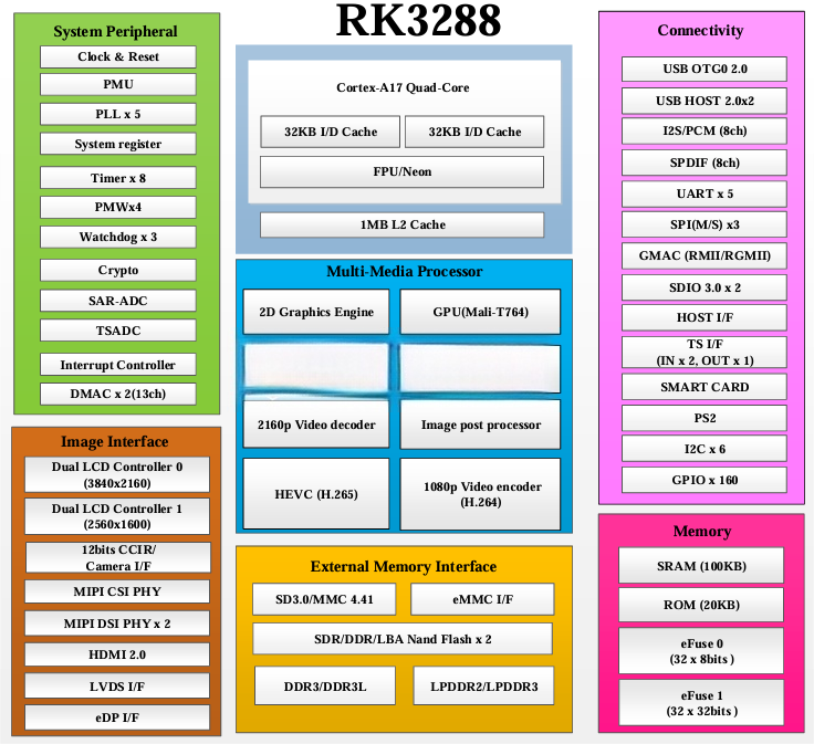
RK3288 Chip Functional Block Diagram:
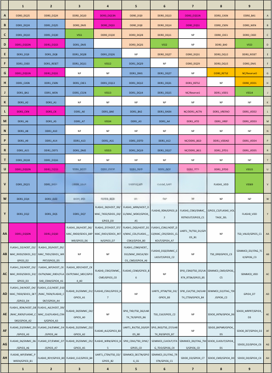
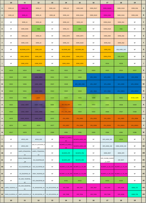
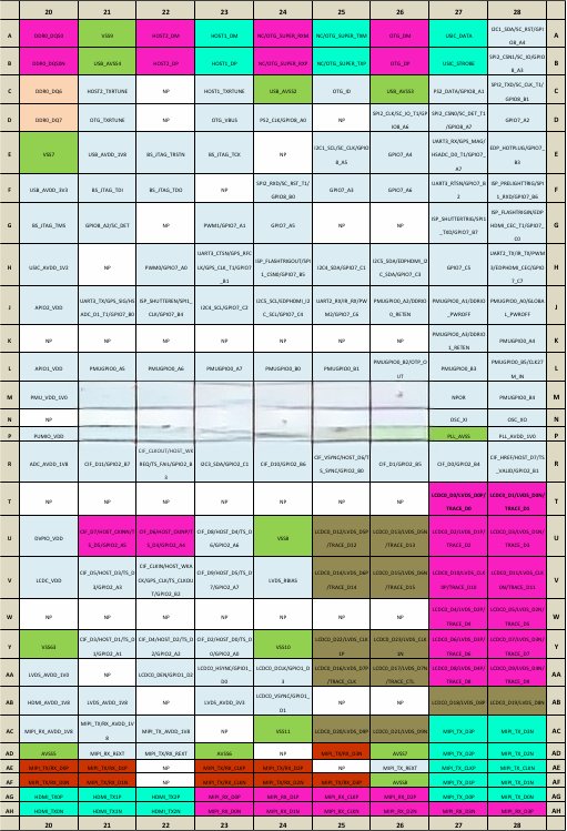
Hi3516CV500 BGA Pin Definition
Partial Schematic Diagram:

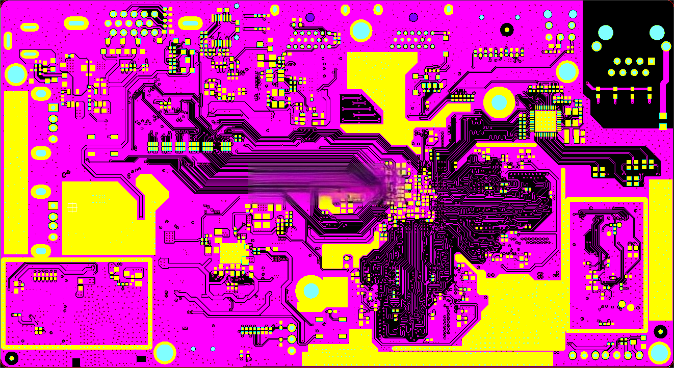
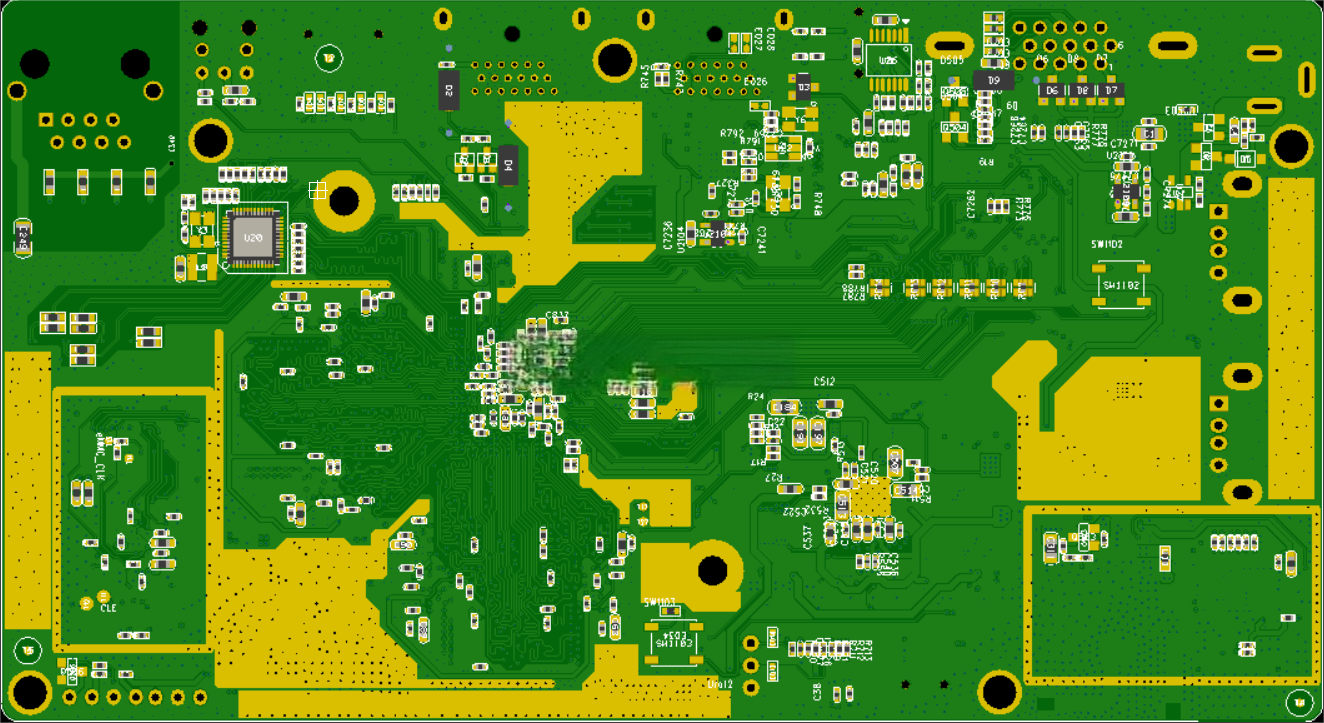
Partial Layout Detail Display
1: The layout of MCU and DDR3 should strictly follow hardware development standards to avoid abnormal data transmission.
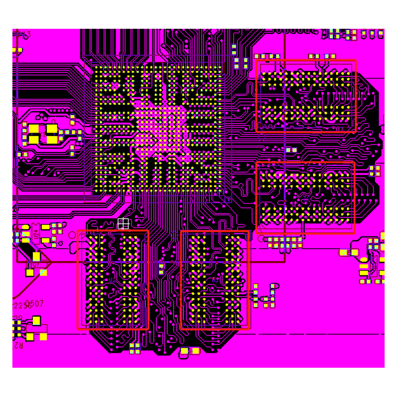
2: Impedance design and signal synchronization need to be considered between MCU and SDA7123.
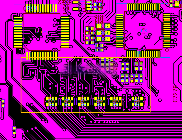
3: Consider comprehensive heat dissipation, set the bottom surface as a large area of GND
PCB Simulation Images:
Top:
Bottom:
Application:
Related Products


-
 Rapid Prototyping
Providing comprehensive one-stop PCB service solutions
-
 Payment
Security
Payment
Security
Multiple payment channels to ensure customer payment security!
-
 Fast
Delivery
Fast
Delivery
Fastest 8 hours, small batch speed 1-2 days
-
 Quality
Assurance
Quality
Assurance
If the quality does not match the description or has defects, we will refund.