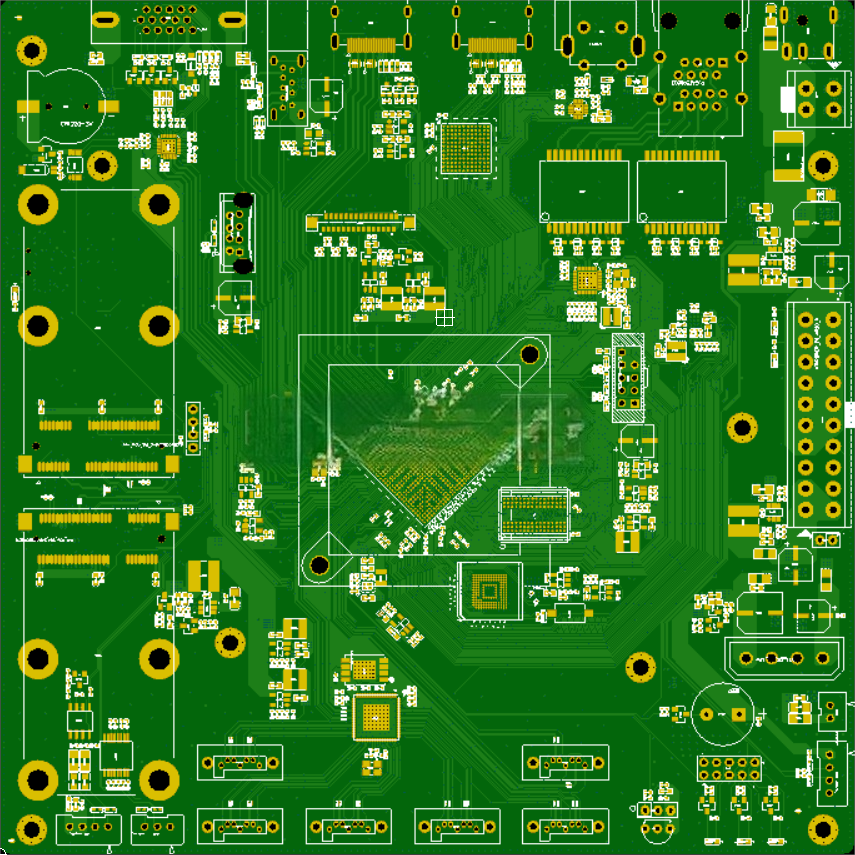
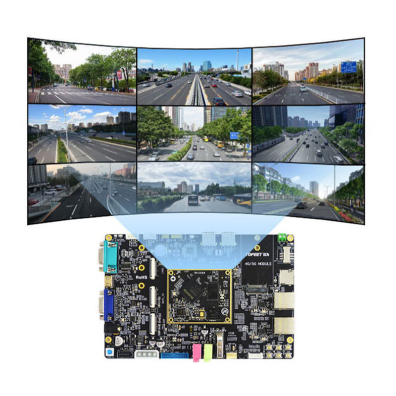
Network video recorder high-speed PCB (RK3568)

Product Name: Rockchip RK3288 Tablet
Industry: Communication Products
Compatible System: Android 10.0
Main Chips: MCU_RK3288, DDR3_128MX16BIT*4 (64G), EMMC, RK1000-S, TC358749XBG, DRV632PW, FT232RL, RK808-B, SDA7123
Board Type: Tablet Computer Motherboard
Application Area: Industrial Tablet Computer
Pin Count: 3717
Layer Number: 6
Board Thickness: 1mm
Dimension: 150*82mm
Line Width/Spacing: 4/4mil
| Product Name | Network Video Recorder High Speed PCB (RK3568) |
| Industry | Communication Products |
| Compatible Systems | |
| Main Chips | RK3568+DDR4+EMMC+RK616+RTD2166+RTL8211F+JMB575+FT232RL |
| Board Type | Computer Motherboard |
| Application Area | Image and Video Capture |
| Layer Number | 4 |
| Board Thickness | 1.2mm |
| Dimension | 170*170mm |
| Line Width/Spacing | 4/4mil |
| Component Quantity | 1171pcs |
| Component Type | 16 |
Design Challenges
1. The layer structure adopts a blind buried hole structure; FPGA adopts blind buried hole wiring;
2. Signal transmission rate 50GB/S, need to consider signal quality and interference;
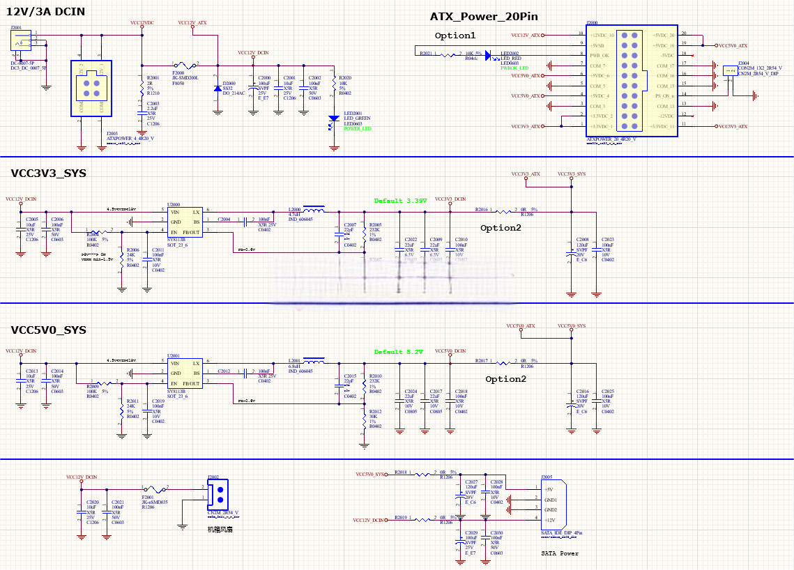
3. DDR, USB, Ethernet, PCIE, SATA, RS485, HDMI wiring all use differential signal wiring, and in order to match impedance, a matching resistance is added between the receiving end differential lines (e.g. SATA differential wiring impedance is 100 ohms. SATA wiring length is less than 5 inches; strictly control line spacing, equidistant;).
4. Distinction between digital power and analog power wiring;
5. Layout of power supply lines (0.9V, 1.8V, 3.3V/500mA, 3.3V/2A, 3.3V/3A, 3.3V/4A, 5V, 12V).
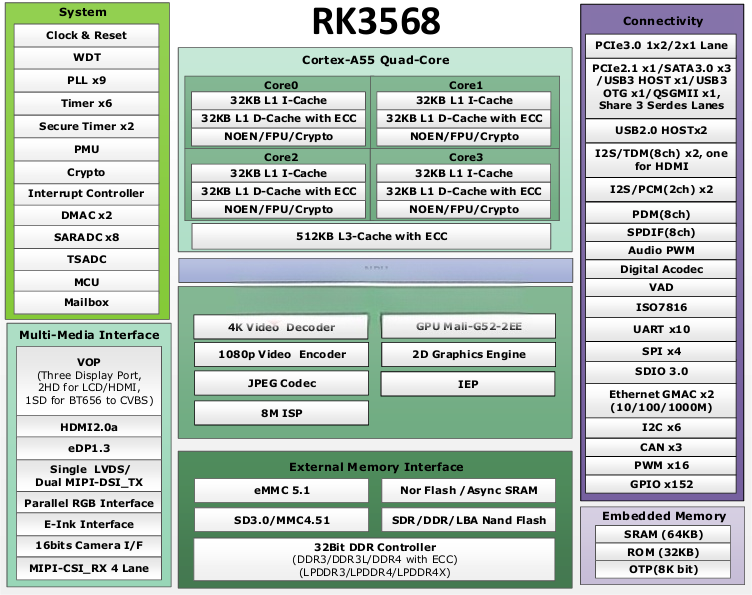
RK3568 Chip Functional Block Diagram :
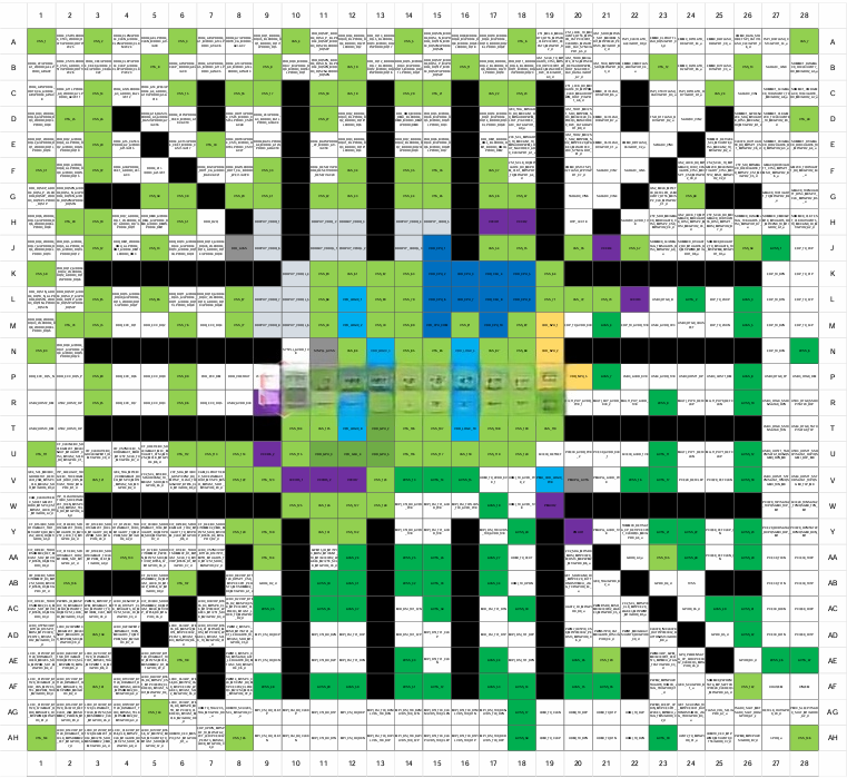
RK3568 BGA Pin Definition:
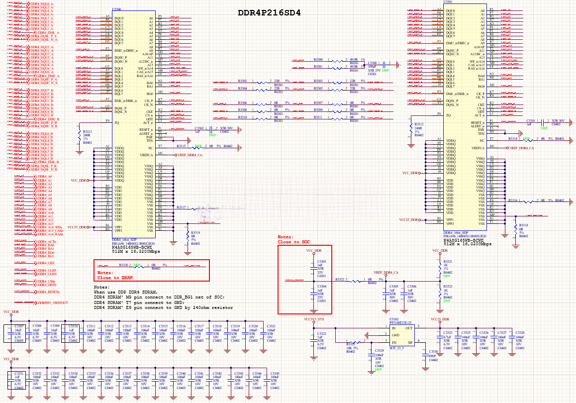
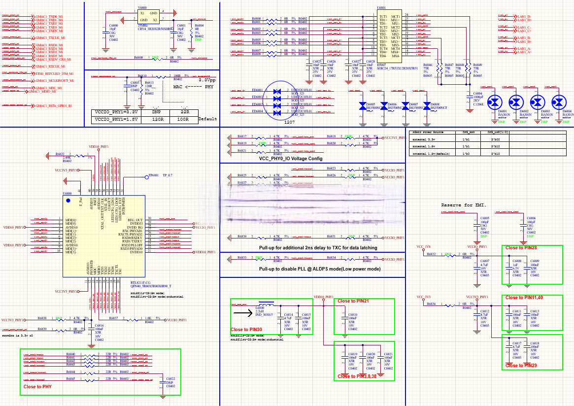
Partial Schematics :
Power Supply Part 1
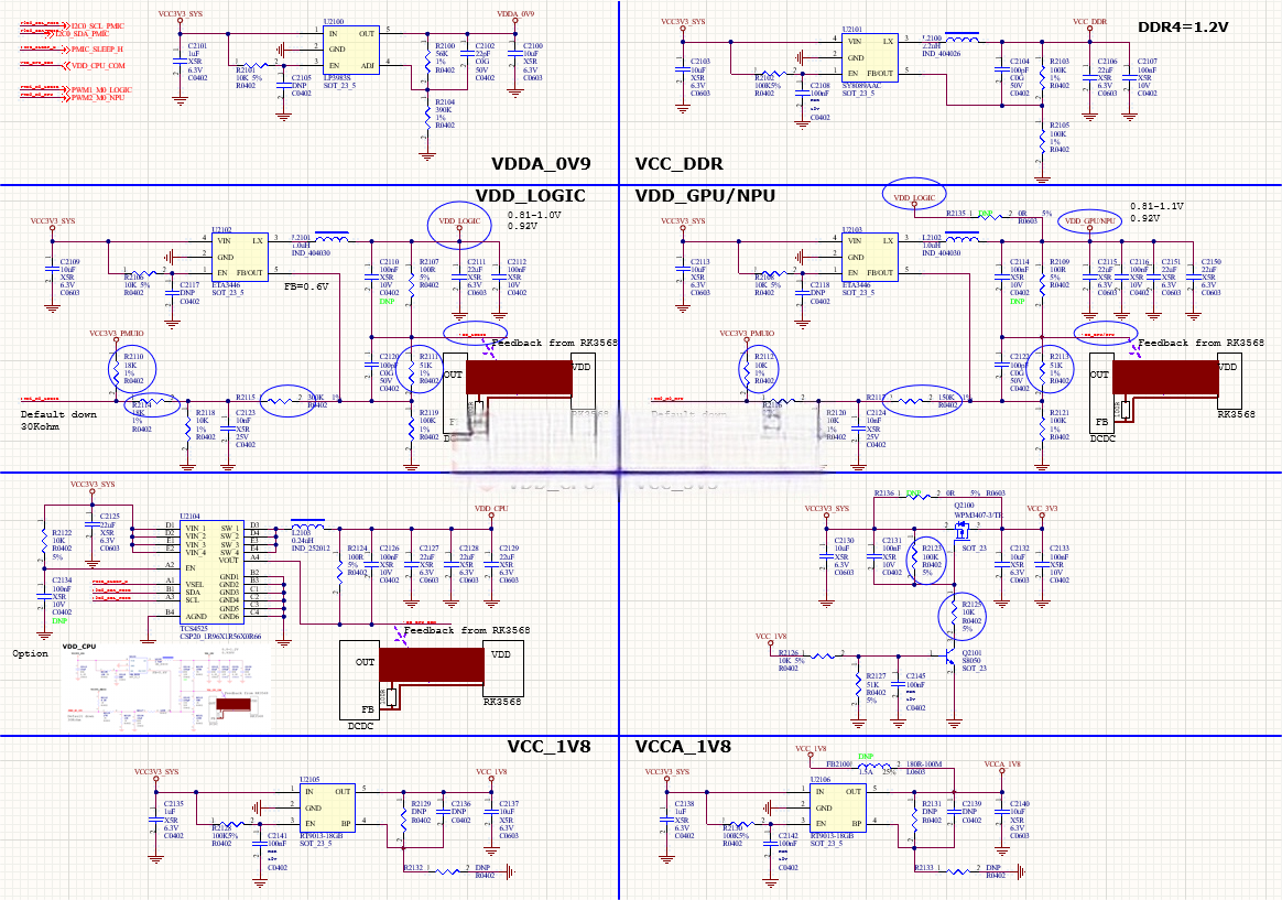
Power Supply Part 2
Power Supply Part 2
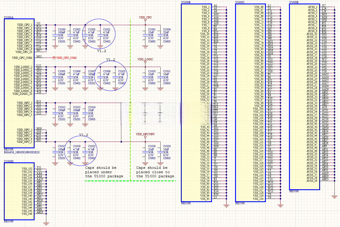
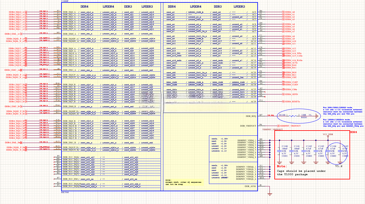
RK3568(DDR PHY)
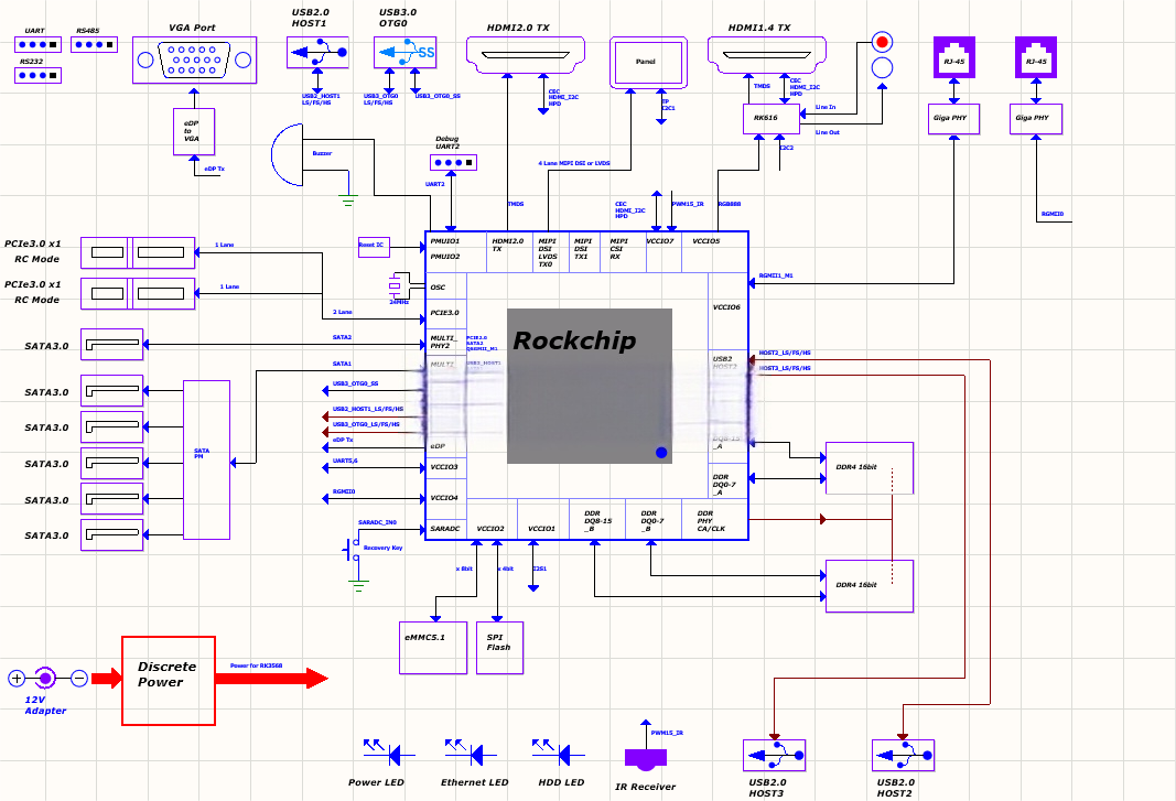
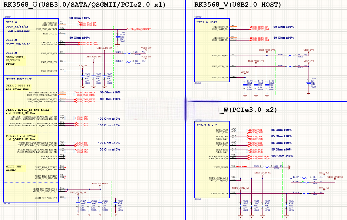
RK3568_U(USB3.0/SATA/QSGMII/PCIe2.0 x1) schematics, pay attention to the green dashed isolation part components, they need to be placed on the back of the PCB layout of RK3568, other components should be placed near the location of RK3568.
DDR4
Ethernet
Some Layout Details Displayed:
1:

2:
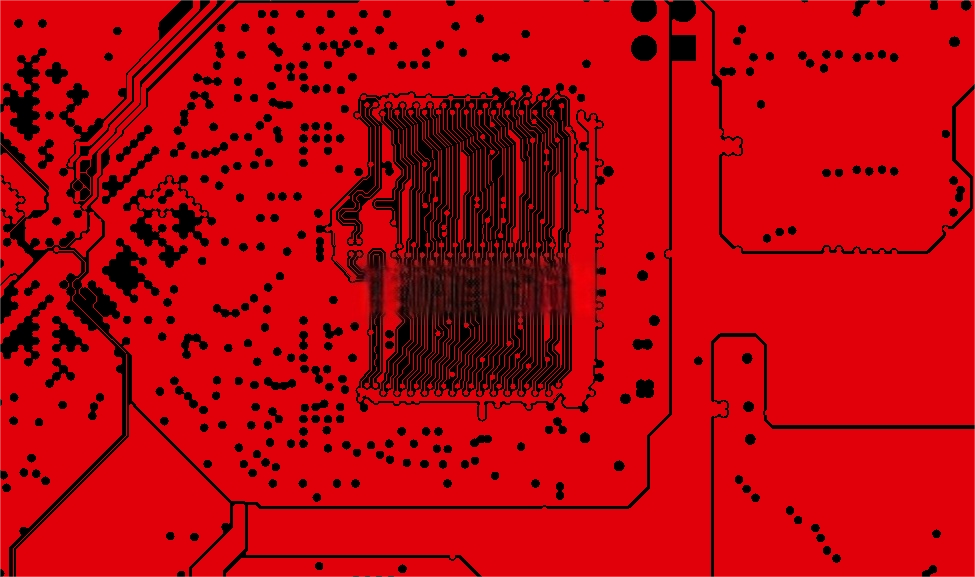
3.
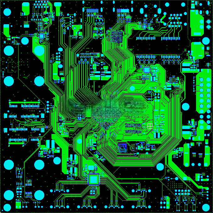
PCB Simulation Diagram :
Application Scenarios

Related Products


-
 Rapid Prototyping
Providing comprehensive one-stop PCB service solutions
-
 Payment
Security
Payment
Security
Multiple payment channels to ensure customer payment security!
-
 Fast
Delivery
Fast
Delivery
Fastest 8 hours, small batch speed 1-2 days
-
 Quality
Assurance
Quality
Assurance
If the quality does not match the description or has defects, we will refund.