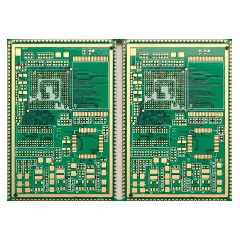
6-layer core board PCB production

Number of layers: 6
Substrate: FR4 Tg150
Board thickness: 1.2mm
Panel size: 118*92mm/10
Outer copper thickness: 35μm
Inner copper thickness: 30μm
Minimum via: 0.20mm
Minimum BGA: 0.25mm
Line width/spacing: 3/3mil
Surface treatment: ENIG 2U"
Special process: 3-side half hole
6-layer core board PCB production
| Number of layers | 6 |
|---|---|
| Substrate | FR4 Tg150 |
| Board thickness | 1.2mm |
| Panel size | 118*92mm/10 |
| Outer copper thickness | 35μm |
| Inner copper thickness | 30μm |
| Minimum via | 0.20mm |
| Minimum BGA | 0.25mm |
| Line width/spacing | 3/3mil |
| Surface treatment | ENIG 2U" |
| Special process | 3-side half hole |
SHC Electronics Limited was founded in 2017 as a high-tech enterprise, specializing in the manufacturing of intelligent controller PCBA, as well as the research, design, and production of intelligent products. We focuses on providing various intelligent controller products and corresponding solutions for industrial controllers, medical products, new energy vehicle electronics, and new smart home applications.
Our factory has obtained certifications such as ISO 9001:2015, ISO 1345:2016, IATF 16949 for automotive, and ISO 13485 for medical quality system certifications. We have the capability to assist customers in completing RoHS and Reach environmental certifications, as well as supporting them in product reliability testing and failure analysis.
Distinguishing itself from factories focused solely on manufacturing, SHC Electronics Limited also provides services such as PCBA design and development, BOM material procurement, DFX evaluation, and other technical support. From the research and development stage to prototyping, small to medium-scale production, and mass production, we provide corresponding manufacturing solutions.
During the product design stage: we can assist with material selection and assist with DFX design, assist with designing the original schematic diagram and Layout design, and the design of test plans. During the sample verification stage, we can provide 10-day fast prototyping, including PCB manufacture, material procurement, and SMT assembly. During the mass production stage, we can assist with mass procurement cost reduction, assist with capacity ramp-up, throughput yield improvement, process failure analysis, verification of key processes, and verification of process parameters.
Related Products


-
 Rapid Prototyping
Providing comprehensive one-stop PCB service solutions
-
 Payment
Security
Payment
Security
Multiple payment channels to ensure customer payment security!
-
 Fast
Delivery
Fast
Delivery
Fastest 8 hours, small batch speed 1-2 days
-
 Quality
Assurance
Quality
Assurance
If the quality does not match the description or has defects, we will refund.